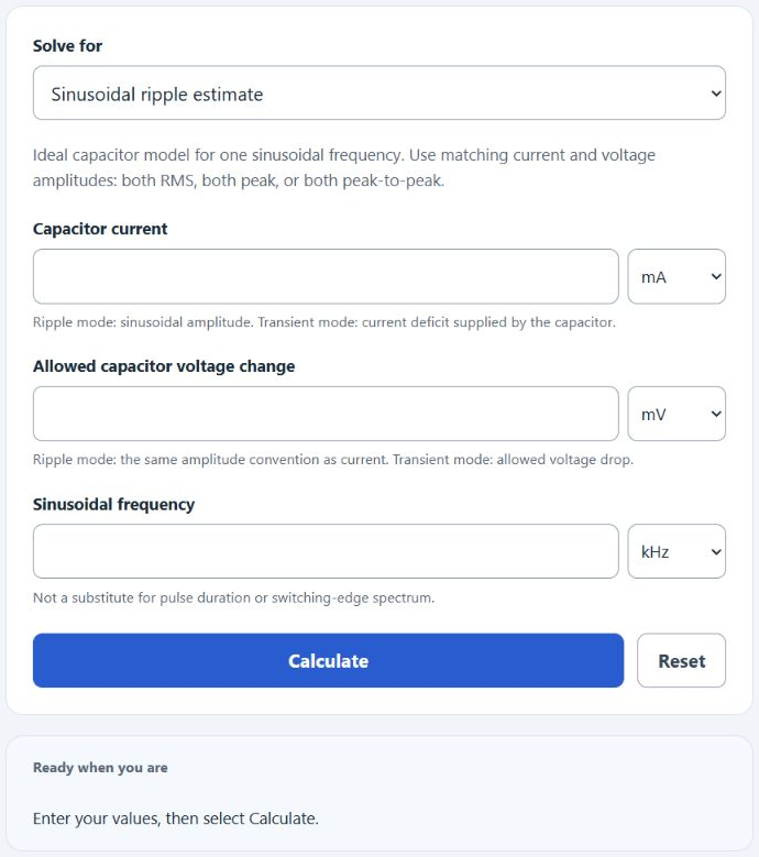
Estimate ideal capacitance for sinusoidal ripple or a constant-current transient, or review illustrative capacitor networks by circuit type. Verify the actual IC datasheet and capacitor impedance before selecting parts.
Related Calculators
- Dielectric Strength Calculator
- Effective Permittivity Calculator
- Heater Resistance Calculator
- Resistor Tolerance Calculator
- All Physics Calculators
Bypass Capacitor Formula
The bypass capacitor calculator uses three approaches: illustrative circuit-type networks, an ideal sinusoidal ripple calculation, or a constant-current charge-storage calculation (C = I × duration / voltage drop).
- C_example = illustrative capacitor network, not a validated IC-specific recommendation
- C = calculated capacitance in farads
- I = sinusoidal capacitor-current amplitude in amps
- f = sinusoidal frequency in hertz
- DeltaV = allowed sinusoidal voltage amplitude in volts, using the same RMS, peak, or peak-to-peak convention as current
- C_std = nearest standard capacitor value at or above the calculated capacitance
- pi = 3.14159…
In the circuit-examples mode, the calculator returns an illustrative network for common IC categories, such as logic gates, microcontrollers, op-amps, RF ICs, and regulators. The legacy example combinations are not validated for every chip in a category; manufacturer requirements take precedence.
The sinusoidal mode uses ideal capacitive reactance; it does not model arbitrary transients. The transient mode instead uses a constant current deficit and its duration. Both return an E12 nominal value at or above the ideal estimate, before derating or stability analysis.
Illustrative Bypass Capacitor Networks by Circuit Type
| Circuit type | Legacy example value | Common note |
|---|---|---|
| Standard digital logic | 0.1 µF | Place one ceramic capacitor close to each VCC pin. |
| Microcontroller | 0.1 µF per VDD pin + 10 µF bulk | Small capacitors handle fast edges, bulk capacitance supports larger load changes. |
| Op-amp | 0.1 µF per supply rail | Bypass both positive and negative rails if the op-amp uses split supplies. |
| High-speed digital or DSP | 0.01 µF + 0.1 µF + 10 µF | Check impedance and possible resonances; parallel values do not guarantee a wider useful range. |
| RF IC | 100 pF + 0.01 µF + 1 µF | Use low-inductance placement and C0G/NP0 for the smallest value. |
| LDO or regulator output | 1 µF to 10 µF | Check the regulator datasheet for stability and ESR requirements. |
Capacitance Range Interpretation
| Calculated range | Possible use; verify impedance | Example capacitor technology |
|---|---|---|
| pF to low nF | Very high-frequency noise or RF bypassing | C0G/NP0 ceramic |
| 10 nF to 1 µF | Local IC decoupling | X7R ceramic |
| 1 µF to 100 µF | Bulk decoupling and load-step support | Ceramic, tantalum, polymer, or electrolytic |
| Above 100 µF | Large current changes or low-frequency ripple | Electrolytic or polymer, often paired with ceramic |
Example Problems
Example 1: Ripple-based bypass capacitor
You have a sinusoidal capacitor current of 100 mA peak, an allowed voltage of 50 mV peak, and a frequency of 100 kHz.
The calculated value is about 3.18 µF. The nearest common standard value above that is 3.3 µF.
Example 2: Microcontroller bypass selection
For a microcontroller, the circuit-examples mode displays this illustrative network:
0.1 µF per VDD pin + 10 µF bulk
The 0.1 µF capacitors should be placed close to the power pins. The bulk capacitor can support slower current changes; follow the particular microcontroller datasheet rather than treating 10 µF as universal.
FAQ
Where should a bypass capacitor be placed?
Place the bypass capacitor as close as practical to the IC power pin it supports. The trace from the power pin to the capacitor and the trace from the capacitor to ground should be short and low-inductance. Poor placement can make a good capacitor value perform badly at high frequency.
Is 0.1 µF always the right bypass capacitor?
No. A 0.1 µF ceramic capacitor is a common starting value for many digital ICs, but it is not universal. High-speed devices, FPGAs, RF ICs, regulators, ADCs, and power circuits may need multiple capacitor values, specific dielectric types, or values specified by the datasheet.
Should you use the exact calculated capacitance?
An E12 nominal value at or above the ideal result is only an initial candidate, not a validated part selection. Real capacitors have tolerance, voltage bias effects, ESR, ESL, and temperature variation. For ceramic capacitors, the actual capacitance can be lower than the label value under DC bias, so using some margin is common.