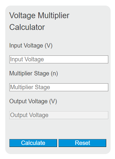
Calculate ideal no-load output voltage, input peak voltage, or multiplier stages for a voltage multiplier from any two known values.
Voltage Multiplier Formula
The following formula is the ideal no-load estimate for a diode-capacitor voltage multiplier chain (commonly modeled as a Cockcroft-Walton multiplier), where each stage contributes approximately 2x the input peak voltage.
Variables:
- Vout is the (ideal, no-load) DC output voltage (V)
- Vpk is the peak value of the AC input voltage (V). For a sine wave, Vpk = sqrt(2) * Vrms.
- n is the number of stages in the voltage multiplier (typically a positive integer)
To estimate the output voltage, multiply twice the input peak voltage by the number of stages. In real designs, the output will be lower under load due to diode forward voltage drops, output ripple, AC source frequency, and capacitor values.
What is a Voltage Multiplier?
A voltage multiplier is an electrical circuit that converts a lower AC input voltage into a higher DC output voltage using only capacitors and diodes, without requiring a step-up transformer. The core principle relies on capacitors being charged in parallel during alternating half-cycles of the AC waveform, then effectively connected in series to deliver their combined voltage to the load. This approach allows circuits to produce output voltages many times greater than the peak input, all from relatively inexpensive, lightweight components.
The concept dates back to 1919 when Heinrich Greinacher built the first cascade voltage doubler. In 1932, John Cockcroft and Ernest Walton famously scaled the design into a multi-stage generator capable of accelerating protons to 700 keV, enabling the first artificial nuclear disintegration of lithium. That experiment earned them the 1951 Nobel Prize in Physics and established the Cockcroft-Walton topology as a foundational tool in high-energy physics. Today, voltage multipliers remain essential wherever high DC voltage at relatively low current is needed, from particle accelerators and X-ray tubes to everyday devices like CRT displays and laser power supplies.
Types of Voltage Multipliers
There are several distinct voltage multiplier topologies, each suited to different voltage ranges, current demands, and integration requirements. Understanding the differences is important for selecting the right circuit for a given application.
Villard Circuit (Half-Wave Clamper)
The simplest voltage multiplier consists of a single capacitor and a single diode. It functions as a DC clamper, shifting the AC waveform upward so the output swings between 0 V and 2Vpk. The Villard circuit is compact and cheap, but its output has very high ripple because no filtering stage is present. It is rarely used alone in precision applications, but it forms the building block of more advanced multipliers.
Greinacher Voltage Doubler
By adding a second capacitor and diode to the Villard circuit as a peak detector stage, the Greinacher doubler produces a DC output of approximately 2Vpk with significantly reduced ripple compared to the Villard alone. Under open-circuit (no-load) conditions, the ripple is nominally zero. Under load, ripple depends on the load resistance, the capacitor values, and the input frequency. The Greinacher doubler is widely used in bench power supplies, CRT anode supplies, and low-power high-voltage applications.
Cockcroft-Walton (CW) Cascade
The Cockcroft-Walton multiplier extends the Greinacher concept into a multi-stage ladder of diodes and capacitors. Each additional stage adds approximately 2Vpk to the output under ideal (no-load) conditions. CW cascades are the dominant topology for generating tens of kilovolts to several megavolts in applications such as particle accelerators, X-ray generators, electrostatic precipitators, and photomultiplier tube power supplies. The key limitation of CW cascades is that voltage drop and ripple both grow rapidly with stage count, which bounds the practical number of stages for a given load current.
Dickson Charge Pump
The Dickson charge pump is a DC-to-DC variant of the voltage multiplier designed specifically for integrated circuits. Instead of an AC sine wave, it uses two antiphase clock signals to shuttle charge through a diode-capacitor chain. Dickson pumps are the standard approach for on-chip voltage boosting in CMOS memory devices (flash EEPROM programming voltages), RFID tags, and energy harvesting circuits. Because the output capacitor must hold the full output voltage, Dickson pumps are best suited to low-voltage, low-current applications (typically under 50 V), unlike CW cascades which distribute the voltage across many capacitors and scale to much higher outputs.
Voltage Drop Under Load
The ideal formula Vout = 2nVpk only applies to an unloaded circuit. When a load draws current, the output voltage drops because each stage’s capacitors must transfer charge through the chain, and higher stages experience progressively greater impedance. For a Cockcroft-Walton multiplier with equal-value capacitors in all stages, the voltage drop is given by:
Where I is the load current in amps, f is the AC input frequency in hertz, C is the capacitance of each stage capacitor in farads, and n is the number of stages. The cubic term (n3) dominates, which means the voltage drop grows very rapidly as stages are added. For example, doubling the number of stages from 4 to 8 increases the voltage drop by roughly a factor of 8, not 2. This cubic scaling is the primary reason why CW multipliers become impractical beyond a certain stage count for any given load current.
The loaded output voltage is therefore:
Where Vd is the forward voltage drop per diode (typically 0.5 to 0.7 V for silicon diodes, or 0.2 to 0.4 V for Schottky diodes). Each stage contains two diodes, but because each diode conducts on only one half-cycle, the net forward drop contribution per stage is approximately one diode drop (Vd) when averaged over the full cycle.
Ripple Voltage
In addition to the DC voltage drop, loaded voltage multipliers exhibit AC ripple on their output. Ripple is the periodic fluctuation in output voltage caused by the capacitors partially discharging into the load between charging cycles. For a CW multiplier with equal capacitors, the peak-to-peak ripple voltage is approximately:
Ripple grows with the square of the number of stages (the n2 term), making it increasingly difficult to maintain a smooth DC output as more stages are added. Higher input frequency and larger capacitance both reduce ripple proportionally. In practical designs, keeping ripple below 1% of the output voltage is a common target, and this constraint often limits the maximum useful stage count more than the voltage drop formula alone would suggest.
Component Selection for Voltage Multipliers
Selecting the right diodes and capacitors directly determines whether a voltage multiplier meets its performance targets. Poor component choices lead to excessive voltage drop, overheating, or premature failure.
Diode Selection
Each diode in the multiplier must be rated for a reverse voltage of at least 2Vpk, regardless of the total output voltage, because individual diodes in a CW cascade never see more than twice the peak input across their terminals. For high-frequency operation (above 20 kHz), fast-recovery or Schottky diodes are preferred because standard silicon rectifiers have reverse recovery times that waste energy and generate heat at elevated switching rates. Schottky diodes also offer a lower forward voltage drop (0.2 to 0.4 V versus 0.5 to 0.7 V for silicon), which directly improves output voltage regulation. For low-current applications (below 1 mA), power dissipation in the diodes is generally negligible. At higher currents, verify that the diode junction temperature stays below the rated maximum (typically 125 to 150 degrees Celsius for silicon devices).
Capacitor Selection
Capacitors must also be rated for at least 2Vpk per stage, since each capacitor in the chain charges to approximately that level. Ceramic capacitors work well for low-capacitance, high-frequency designs. Film capacitors (polypropylene or polyester) are preferred for higher capacitance values and better voltage handling. Electrolytic capacitors can be used in low-voltage stages but are generally avoided in high-voltage multiplier designs because of their lower voltage ratings and polarity requirements. Larger capacitance values reduce both voltage drop and ripple but increase physical size and cost. A common design starting point is to choose C such that the time constant (1/fC) is at least 10 times the load discharge period.
Applications of Voltage Multipliers
Voltage multipliers serve a wide range of industries. In medical imaging, X-ray tubes require 30 kV to 150 kV DC, commonly generated by CW cascades driven at 20 kHz to 100 kHz from inverter-fed transformers. Particle accelerators still use CW generators at facilities worldwide, producing voltages from 500 kV up to several MV for ion beam research. Electrostatic precipitators in coal-fired power plants use multipliers to generate the 20 kV to 100 kV DC fields needed to ionize and capture particulate emissions.
At lower voltage scales, photomultiplier tubes in nuclear medicine (PET and SPECT scanners) and high-energy physics detectors require stable 1 kV to 2 kV supplies that CW multipliers provide compactly. Laser systems, including CO2 industrial cutting lasers and excimer lasers for semiconductor lithography, use multipliers for their gas discharge power supplies. In consumer electronics, CRT television sets historically used voltage triplers to generate the 25 kV to 30 kV anode voltage, and modern LCD backlighting with CCFL tubes uses small multiplier circuits for the 1 kV to 1.5 kV strike voltage. Copy machines and laser printers use corona wire multipliers at 5 kV to 7 kV for electrostatic charging of the drum. Air ionizers and electrostatic air cleaners rely on multipliers operating in the 3 kV to 10 kV range.
On the integrated circuit side, Dickson charge pumps generate the 10 V to 20 V programming voltages for flash memory (NAND and NOR) from 1.8 V to 3.3 V supply rails. RFID tags use on-chip charge pumps to rectify and boost the received RF energy to usable logic levels. Energy harvesting circuits in IoT sensors similarly employ charge pumps to step up the millivolt-level outputs from thermoelectric generators or piezoelectric transducers to the 1.8 V or 3.3 V needed by microcontrollers.
Design Optimization Techniques
Several strategies can improve the performance of a voltage multiplier beyond the basic equal-capacitor design. Graded capacitance is the most impactful: instead of using the same capacitor value in every stage, the bottom (closest to the input) stages use larger capacitors and the upper stages use smaller ones. The standard grading scheme sets C1 and C2 = nC, C3 and C4 = (n-1)C, and so on, where C is a base capacitance. This equalizes the charge transfer per stage and reduces voltage drop by roughly 50% compared to equal capacitors at the same total capacitance budget.
Increasing the input frequency is another highly effective technique. Both voltage drop and ripple are inversely proportional to frequency, so moving from a 50/60 Hz mains supply to a 20 kHz or higher switching supply reduces both by a factor of 300 to 400. This is why modern high-voltage power supply designs almost universally use a high-frequency inverter stage before the multiplier. The tradeoff is that diode reverse recovery losses increase with frequency, requiring the use of fast-recovery or Schottky diodes above roughly 20 kHz.
Symmetrical (full-wave) multiplier topologies drive the capacitor ladder from both halves of the AC cycle simultaneously. This effectively doubles the charging frequency seen by the capacitors, cutting ripple and voltage drop in half for the same component values. Full-wave designs require a center-tapped or dual-output AC source but are standard practice in professional high-voltage supplies.
Voltage Multiplier Topology Comparison
The following comparison summarizes the practical characteristics of each major multiplier type to aid in selecting the right topology for a given design requirement.
| Topology | Typical Output Range | Ripple | Best For |
|---|---|---|---|
| Villard (single diode-cap) | Up to 2Vpk | High | Simple DC level shifting, bias circuits |
| Greinacher Doubler | Up to 2Vpk | Low (open-circuit) | Bench supplies, CRT anodes, low-power HV |
| Cockcroft-Walton Cascade | kV to MV range | Moderate (grows with n2) | X-ray, particle accelerators, precipitators |
| Dickson Charge Pump | Under 50 V (typically) | Low (clock-controlled) | On-chip CMOS, flash memory, RFID, energy harvesting |