Calculate SIW effective width, TE10 cutoff frequency, or required via-row spacing from via geometry, substrate permittivity, and target GHz.
Customize This Calculator
Build your own version. Describe what you want changed, added, or compared.
- All Unit Converters
- Bandpass Filter Calculator
- Resonant Frequency Calculator
- SWR Calculator
- dB to SWR Converter
- Maximum Usable Frequency Calculator
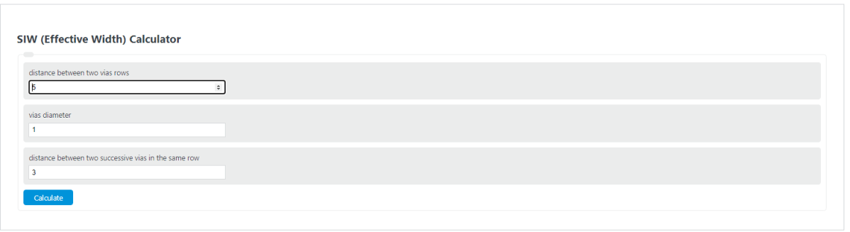
SIW Effective Width Formula
The effective width of a substrate integrated waveguide is calculated using the following empirical relationship, which maps the SIW geometry to an equivalent rectangular waveguide width:
- W_eff is the effective width of the equivalent rectangular waveguide
- a is the center-to-center distance between the two rows of metallized vias
- d is the diameter of each metallized via
- s is the center-to-center pitch (spacing) between consecutive vias in the same row
This formula was derived empirically by comparing the dispersion characteristics of SIW structures to those of dielectric-filled rectangular waveguides. The correction term accounts for the electromagnetic field leakage that occurs between the discrete via posts, which makes the effective guiding width narrower than the physical via row spacing. Once the effective width is known, the TE10 cutoff frequency of the SIW can be found using the standard rectangular waveguide cutoff equation: f_c = c / (2 * W_eff * sqrt(er)), where c is the speed of light in vacuum and er is the relative permittivity of the substrate.
What Is a Substrate Integrated Waveguide (SIW)?
A substrate integrated waveguide is a planar electromagnetic guiding structure that replicates the behavior of a conventional rectangular waveguide entirely within a printed circuit board (PCB) substrate. Two rows of densely spaced metallized via holes connect the top and bottom copper layers of the PCB, forming the sidewalls of the waveguide. The top and bottom copper planes serve as the broad walls. The result is a closed, shielded transmission line that supports the same TE mode family as a classical rectangular waveguide, but in a flat, mass-producible form factor compatible with standard PCB and low-temperature co-fired ceramic (LTCC) fabrication processes.
The concept was first formalized in the early 2000s by Ke Wu and Dominic Deslandes at the Ecole Polytechnique de Montreal, though earlier related work on laminated waveguides dates to the 1990s. Their key insight was that two rows of periodic metallic posts, when spaced closely enough relative to the operating wavelength, behave nearly identically to solid metallic sidewalls. This allowed engineers to bring waveguide-class performance (high Q-factor, low radiation loss, high power handling) into the same multilayer PCB stack-ups already used for microstrip and stripline circuits.
SIW Structure and Operating Principle
The physical structure of a SIW consists of four elements: a dielectric substrate layer, two parallel copper ground planes (top and bottom), and two linear arrays of plated-through vias drilled through the substrate connecting the ground planes. The electromagnetic wave propagates through the dielectric material between the via rows, confined laterally by the vias and vertically by the copper planes.
Only transverse electric (TE) modes propagate in a SIW. The dominant mode is TE10, identical to the fundamental mode of a rectangular waveguide. Transverse magnetic (TM) modes and TEM modes cannot exist because the via walls are not continuous conductors in the longitudinal direction, and the boundary conditions required for TM mode support are not satisfied by the periodic post structure. This single-mode behavior is actually an advantage in many filter and antenna designs, as it simplifies the mode spectrum and avoids spurious resonances that can appear in oversized rectangular waveguides.
Because the via posts are discrete rather than continuous, the SIW is slightly wider than the equivalent rectangular waveguide that would produce the same cutoff frequency. The effective width formula above quantifies this difference. For a well-designed SIW with recommended via sizing, the effective width is typically 90% to 98% of the physical via row spacing, depending on the d/s ratio.
Critical Design Rules
Three geometric constraints must be satisfied for a SIW to function properly with low radiation loss. First, the via pitch must remain small relative to the via diameter: s/d should be kept below 2.5, with an optimum near s = 2d. When the pitch-to-diameter ratio exceeds roughly 2.5, the gaps between vias become electrically large enough for significant energy leakage, degrading both insertion loss and isolation. Second, the via diameter itself must be electrically small relative to the guided wavelength: d should be less than approximately one-fifth of the guided wavelength (d less than 0.2 times the guided wavelength). This ensures the vias behave as an effective conducting wall rather than individual scatterers. Third, the waveguide width (a) must be chosen so the operating frequency band falls between the TE10 cutoff and the TE20 cutoff, maintaining single-mode propagation.
As a practical numerical example, a SIW designed for 28 GHz operation on Rogers RT/Duroid 5880 (er = 2.2) would require an effective width near 3.6 mm to place the TE10 cutoff around 28 GHz. With 0.4 mm diameter vias at 0.8 mm pitch, the physical via row spacing would be approximately 3.8 mm, and the via diameter satisfies d divided by the guided wavelength of approximately 0.06, well within the recommended limit.
Loss Mechanisms in SIW
Three distinct loss mechanisms affect SIW performance, and understanding their relative contributions is important for design optimization at different frequency bands.
Conductor loss arises from the finite conductivity of the copper ground planes and via walls. It follows the same skin-depth scaling as in conventional waveguides: loss increases with the square root of frequency. Using thicker substrates reduces conductor loss because the current density spreads over a larger surface area. At frequencies below roughly 30 GHz, conductor loss is typically the dominant loss contributor in a well-designed SIW.
Dielectric loss comes from the substrate material's loss tangent (tan delta). Unlike air-filled rectangular waveguides that have zero dielectric loss, SIW structures are entirely filled with dielectric, so this term is always present. It scales linearly with frequency and with the loss tangent value. At millimeter-wave frequencies above 40 GHz, dielectric loss often overtakes conductor loss, which is why low-loss substrates like Rogers RT/Duroid 5880 (tan delta = 0.0009) are strongly preferred over standard FR-4 (tan delta of approximately 0.02) for high-frequency SIW designs.
Radiation loss is unique to SIW and results from electromagnetic energy leaking through the gaps between adjacent vias. This loss can be made negligibly small by following the design rules above (s/d below 2.5, d less than one-fifth of the guided wavelength). When those constraints are met, radiation loss contributes less than 0.01 dB per guided wavelength, which is insignificant compared to the conductor and dielectric terms.
Common Substrate Materials for SIW
The choice of substrate material directly impacts the SIW's cutoff frequency (through the dielectric constant), its loss performance (through the loss tangent), and its manufacturability. The table below lists materials commonly used in published SIW designs, along with their key electrical properties at 10 GHz.
| Material | Dielectric Constant (at 10 GHz) | Loss Tangent | Typical Use Case |
|---|---|---|---|
| Rogers RT/Duroid 5880 | 2.20 | 0.0009 | Ka-band and W-band SIW filters, antennas |
| Rogers RT/Duroid 5870 | 2.33 | 0.0012 | Satellite communication SIW arrays |
| Rogers RO4350B | 3.48 | 0.0037 | Cost-sensitive microwave SIW circuits |
| Rogers RO4003C | 3.55 | 0.0027 | General microwave, moderate loss tolerance |
| Isola Astra MT77 | 3.00 | 0.0017 | 5G mmWave front-end modules |
| Taconic TLY-5 | 2.20 | 0.0018 | Alternative to RT/Duroid 5880 |
| FR-4 (standard) | 4.30 | 0.020 | Low-frequency SIW prototyping (below 6 GHz) |
A lower dielectric constant means a physically wider SIW for a given cutoff frequency, but it also means lower dielectric loss. RT/Duroid 5880 is the most widely cited substrate in SIW research literature because its combination of er = 2.2 and extremely low loss tangent (0.0009) provides excellent performance through Ka-band (26.5 to 40 GHz) and into W-band (75 to 110 GHz). The dielectric constant of RT/Duroid 5880 remains remarkably stable, varying only from 2.22 to 2.18 across the range from 1 MHz to 40 GHz. For cost-constrained commercial applications below 10 GHz, FR-4 remains viable despite its high loss tangent, since the dielectric loss contribution is proportionally smaller at lower frequencies.
SIW vs. Microstrip vs. Rectangular Waveguide
SIW technology occupies a unique middle ground between traditional planar transmission lines (microstrip, stripline, coplanar waveguide) and conventional air-filled rectangular waveguide. Understanding where each technology excels helps engineers select the right guiding structure for a given application.
Microstrip is the simplest and cheapest planar transmission line, supporting quasi-TEM propagation from DC through roughly 10 GHz with acceptable loss. Above 10 GHz, microstrip suffers from increasing radiation loss, surface wave excitation into the substrate, and difficulty maintaining tight impedance tolerances as line widths shrink. Typical microstrip insertion loss at 30 GHz is approximately 0.5 dB/cm on standard substrates, which becomes prohibitive for complex filter or beamforming networks.
Air-filled rectangular waveguide offers the lowest possible insertion loss (below 0.05 dB per meter at X-band) and can handle kilowatts of power. However, it is a bulky, three-dimensional machined structure that cannot be integrated onto a PCB. Connections between waveguide sections require precision flanges, and the manufacturing cost per unit is high.
SIW provides waveguide-class Q-factors (typically 150 to 500 depending on frequency and substrate) in a PCB-compatible package. It can be fabricated using the same drilling, plating, and etching processes already present in any PCB factory, with no special tooling. The unloaded Q-factor of an SIW resonator is roughly 5 to 10 times higher than a microstrip resonator at the same frequency, which translates directly to sharper filter skirts and lower oscillator phase noise. The tradeoff is that SIW has higher loss than air-filled waveguide (due to the dielectric fill) and occupies more board area than microstrip for the same frequency.
Applications of SIW Technology
SIW has become a foundational building block for microwave and millimeter-wave circuits across several industries. In 5G wireless infrastructure, SIW-based bandpass filters and antenna feed networks operate in both the sub-6 GHz bands (3.5 GHz, 4.9 GHz) and the millimeter-wave bands (28 GHz, 39 GHz). The self-shielding property of SIW is particularly valuable in dense 5G front-end modules where multiple filters and amplifiers share a single PCB and electromagnetic interference between channels must be minimized.
Automotive radar systems at 77 GHz and 79 GHz use SIW slot antenna arrays to achieve the narrow beamwidths needed for long-range object detection while fitting within the constrained packaging behind a vehicle bumper. SIW cavity-backed slot antennas at these frequencies achieve gains of 6 to 12 dBi from a single element, and arrays of 8 to 16 elements reach 15 to 20 dBi, sufficient for medium-range radar at distances of 30 to 80 meters.
Satellite communication systems use SIW for Ka-band diplexers and multiplexers that separate transmit (27.5 to 31 GHz) and receive (17.7 to 21.2 GHz) paths on the same antenna panel. The high Q-factor of SIW resonators enables steep roll-off between closely spaced bands without the bulk and cost of machined waveguide diplexers. Published SIW diplexer designs on RT/Duroid 5880 demonstrate channel isolation above 40 dB with insertion loss below 0.8 dB.
In scientific instrumentation, SIW is used to build compact six-port reflectometers and directional couplers for material characterization and dielectric sensing. The enclosed structure provides excellent repeatability and shielding from external interference, making SIW sensors suitable for inline industrial monitoring of moisture content, liquid permittivity, and material thickness at microwave frequencies.