Calculate gross and good dies per wafer from wafer size, die dimensions, edge exclusion, and defect density using Poisson or Murphy yield.
- Total Manufacturing Cost Calculator
- Direct Labor Costs Calculator
- PPM Calculator
- Blow Up Ratio Calculator
- All Math and Numbers Calculators
- Casting Yield Calculator
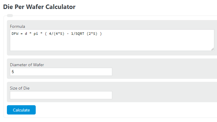
Die Per Wafer Formula
The calculator uses three formulas depending on which tab you choose.
Gross dies per wafer (Dimensions and Die area tabs):
- DPW = gross dies per wafer
- d = usable wafer diameter (wafer diameter minus 2 × edge exclusion), in mm
- A = die footprint area (die width + street) × (die height + street), in mm²
Poisson yield (Good dies tab):
Murphy yield (Good dies tab):
- Y = die yield (fraction of good dies)
- D0 = defect density, in defects/cm²
- A = die area, in cm²
Expected good dies = gross DPW × Y. The gross formula is the standard area-minus-edge-loss approximation; it does not account for flat or notch placement, reticle stepping, or partial die exclusions, so real fab numbers may differ by a few percent.
Reference Tables
Typical wafer areas before edge exclusion:
| Wafer diameter | Area (mm²) | Area (cm²) |
|---|---|---|
| 100 mm | 7,854 | 78.5 |
| 150 mm | 17,671 | 176.7 |
| 200 mm | 31,416 | 314.2 |
| 300 mm | 70,686 | 706.9 |
| 450 mm | 159,043 | 1,590.4 |
Typical defect densities by process maturity:
| Process state | D0 (defects/cm²) |
|---|---|
| Mature CMOS, high-volume node | 0.05 – 0.15 |
| Established node, normal production | 0.15 – 0.30 |
| New node ramp | 0.30 – 0.80 |
| Early development / R&D | 1.0 – 2.0+ |
Worked Example
A 300 mm wafer with 5 mm edge exclusion, 10 mm × 10 mm die, and 0.1 mm scribe street per side:
- Usable diameter: 300 − 2(5) = 290 mm
- Die footprint: 10.1 × 10.1 = 102.01 mm²
- Area-only maximum: π(290)² / (4 × 102.01) ≈ 647 dies
- Edge-loss term: π(290) / √(2 × 102.01) ≈ 64 dies
- Gross DPW ≈ 583
If defect density is 0.2/cm² with Poisson yield: Y = exp(−0.2 × 1.0201) ≈ 0.816, so expected good dies ≈ 475.
FAQ
Why is my answer lower than (wafer area / die area)? Rectangular dies cannot tile a circular wafer perfectly. The √(2A) term subtracts the dies lost along the curved edge.
Poisson or Murphy? Poisson assumes uniform defect distribution and tends to underestimate yield for large dies. Murphy assumes a Gaussian-like spread of defect density across the wafer and is closer to real data for dies above roughly 1 cm².
What should I use for scribe street? 50 to 100 µm per side is typical for modern processes. Set it to zero if your die dimensions already include the kerf.
What is edge exclusion? The outer ring of the wafer where dies are not patterned because of handling damage or process non-uniformity. 3 to 5 mm is common.